Javier Sanchez-Yamagishi, Thiti Taychatanapat, Leonardo Campos, Joel Wang
Unlike any other material, Graphene is all surface. Its atoms are completely exposed to its environment without any interior bulk. What this means in practice is that graphene is often strongly affected by its surroundings, even by the substrate it lays upon. Today, it’s now understood that silicon dioxide, the most common substrate material for graphene, limits the performance of graphene devices and obscures interesting physics. This is thought to be caused by the roughness of the SiO2 substrates, which induce corrugations in the graphene, as well as charge traps in the SiO2 which results in inhomogeneous doping.
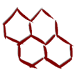
In the Jarillo-Herrero group we are exploring a newly discovered substrate material -hexagonal boron nitride- which addresses the issues with SiO2 and results in greatly improved graphene devices. Hexagonal boron nitride (hBN) turns out to be the perfect match for graphene because they share many similarities. hBN is just graphene with the carbon atoms replaced by boron and nitrogen resulting in the same honeycomb lattice with the bulk crystal forming a layered structure similar to graphite. The key difference is that hBN is a large bandgap semiconductor (Eg ~5ev) and hence is an insulator and can serve as a substrate material. hBN can be exfoliated just like graphite, resulting in atomically smooth layers which are ultra-flat. In addition, because of its planar structure and high purity there are few dangling bonds or charge traps to interfere with the properties of a graphene layer which is placed on top of the hBN.


