Javier Sanchez-Yamagishi, Ken Van Tilburg, Danny Bulmash

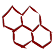
Ni nanoparticles etch SLG along a crystallographic axis
When graphene is confined to a nanoribbon a transport gap is opened which allows for field effect transistor operation. Such graphene nanoribbon FETs have been demonstrated, but are thought to be dominated by edge disorder and hence operate far from the the intrinsic regime. More generally, graphene edge structure are predicted to have a strong effect on the electrical, chemical and magnetic properties of graphene structures. Experimentally, these effects have been difficult to verify since standard nanofabrication methods produce disordered graphene edges.
This project investigates methods of fabricating graphene nanostructures with edges defined along graphene’s crystallographic axis and to study edge-effects on graphene’s electronic transport.
Our current method uses Ni nanoparticles which preferentially cut graphene along crystallographic directions, unlike the randomly orientated edges produced by standard plasma etching process. At high temperatures under H2 flow, these Ni nanoparticles being to eat the graphene (like pacman), moving across the graphene surface as it removes carbon. The etching Ni nanoparticles also avoid intersecting other cuts during the etching process, naturally producing nanoribbons. The resulting nanoribbons are aligned with graphene’s crystallographic axis and should feature novel transport behavior.
-

- Ni nanoparticles etch SLG along a SINGLE crystallographic axis


-

- Crystallographic Cuts in Graphene


-

- Crystallographic cuts in FLG show up with high contrast in SEM

Relevant Publications
Anisotropic etching and nanoribbon formation in single-layer graphene.
Leonardo C. Campos, Vitor R. Manfrinato, Javier D. Sanchez-Yamagishi, Jing Kong, Pablo Jarillo-Herrero (2009)
Nano letters 9 (7) p. 2600–2604
http://dx.doi.org/10.1021/nl900811r