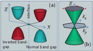
Topological Insulators are materials where the band-structure has a bulk band-gap but unusual quantum states are expected to exist at the surface. These so-called topological surface states appear as a result of a role switching between the conduction and valence bands across an interface (Figure 1a). The surface states are characterized by a linear dispersion, similar to graphene (Figure 1b), but are topologically protected due to underlying symmetries of the bulk band-structure.
Some of the most interesting predictions about topological insulators arise when considering their interface to superconductors. Under fine-tuned conditions, the interface is expected to host quantum states called “Majorana Bound States”, which are characterized by non-Abelian statistics. These states are one of the holy-grails of condensed matter physics, since they may form the foundation to fault-tolerant quantum computation schemes.
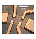
We study the properties of the topological surface states using low-temperature electronic transport measurements. We use the topological insulator Bi2Se3 which we synthesize by melting the constituent components in a heated quartz tube, and use electron beam lithography to contact exfoliated flakes – similar to the technique used for graphene devices. Figure 2 is an AFM image of one of our devices.
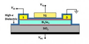
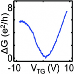
By applying a top-gate electrode (see schematic in Figure 3), we are able to control the surface carrier density. This is a desired property, since it paves the way for future applications which utilize the special topological properties of the surface state, where density control is required. In Figure 4 we plot the conductance of the device with application of the top gate. The conductance increases when applying a positive gate voltage, and also when applying a negative gate voltage. This is an indication of a transition between negative and positive charge carriers, and confirms that the gate voltage modulates the Dirac dispersion of the top surface state. The conductance minimum is found when the Dirac point is tuned through the Fermi energy.


